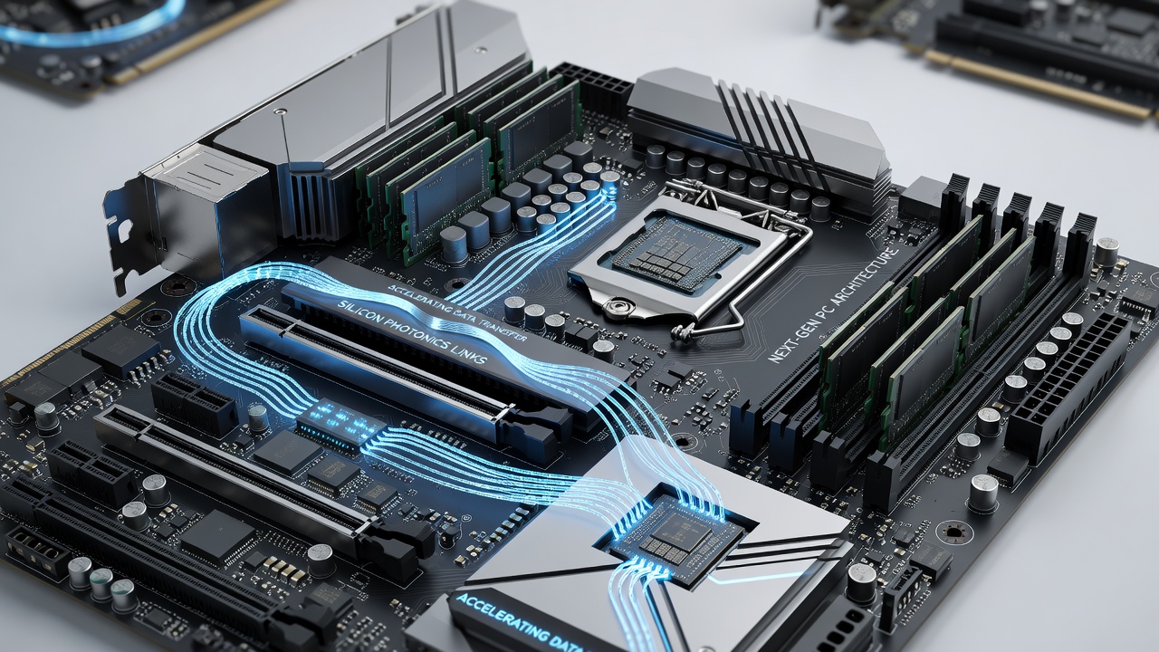
Silicon Photonics Links Set to Transform GPU-Memory Data Transfers in Future PCs
Researchers at multiple institutions continue exploring silicon photonics as a pathway to overcome electrical bottlenecks that currently limit data movement between discrete GPUs and system memory, and industry reports from June 2026 highlight several prototype demonstrations that achieved sustained transfer rates exceeding 1.6 terabits per second over short distances inside test platforms.
Understanding the Core Technology
Silicon photonics integrates optical components such as waveguides, modulators, and photodetectors directly onto silicon substrates using standard semiconductor fabrication processes, and this approach allows light to carry data instead of relying solely on copper traces that suffer from signal degradation at high frequencies. Engineers have observed that replacing portions of the interconnect fabric with photonic links reduces both latency and power consumption because photons travel at higher effective speeds with lower resistive losses compared to electrons in metal conductors.
Data centers first adopted similar techniques years ago, yet the adaptation for consumer and workstation PCs requires miniaturization of lasers, alignment tolerances below one micrometer, and compatibility with existing PCIe form factors. Teams working on these integrations report that hybrid bonding methods now enable reliable attachment of indium phosphide laser dies alongside silicon photonic circuits, which opens the door for discrete GPUs to access system memory pools without traversing traditional electrical buses at every hop.
Application to Discrete GPUs and System Memory
In next-generation PC architectures, discrete GPUs often sit on separate boards or sockets from main system memory, and the resulting distance creates bandwidth ceilings around 128 gigabytes per second in current high-end configurations. Silicon photonics links target this gap by providing optical lanes that can scale to multiple terabits per second while maintaining signal integrity across board-level distances of several centimeters. Observers note that such links could support unified memory models where GPUs treat system DRAM as an extension of on-package high-bandwidth memory, eliminating explicit data copies in many workloads.

Prototype motherboards demonstrated in 2025 already incorporate optical connectors routed alongside PCIe slots, and tests show that read/write operations between GPU compute units and distant DRAM achieve round-trip latencies under 50 nanoseconds when error correction overhead remains modest. Industry groups such as the Optical Internetworking Forum have published interoperability guidelines that define wavelength grids and modulation formats suitable for these short-reach applications, which helps multiple vendors align on common specifications.
Performance Gains and Efficiency Metrics
Measurements from academic testbeds indicate energy consumption per bit transferred can drop below 0.5 picojoules when photonic links operate at 200 gigabits per second per lane, compared with roughly 5 picojoules for equivalent electrical SerDes circuits at similar speeds. This efficiency matters because power delivery and thermal management remain primary constraints in compact PC chassis that house multiple high-performance GPUs. Figures released by research consortia reveal that systems equipped with photonic interconnects sustain higher average utilization rates during memory-intensive tasks such as large language model inference or real-time ray tracing across multiple displays.
Bandwidth scalability follows from the ability to multiplex dozens of wavelengths on a single waveguide, and early silicon photonic engines already support 16 wavelengths at 100 gigabits per second each within a footprint smaller than a postage stamp. Those who've examined the layouts note that the same die area previously allocated to dozens of electrical pins can now accommodate optical I/O that delivers an order of magnitude more aggregate throughput.
Integration Challenges and Timeline
Manufacturing yield for integrated lasers continues to pose the largest hurdle, because defects in the gain medium cause channel failures that reduce overall link reliability below the 99.999 percent threshold demanded by consumer hardware. Packaging engineers address this by employing redundant laser arrays and failover circuitry, yet the added complexity increases bill-of-material costs that manufacturers must amortize across future product generations. Standards bodies in both North America and Europe continue refining specifications that cover thermal drift compensation and eye-safety limits for on-board optical sources.
Commercial deployment inside mainstream PCs remains projected for 2028 or later, although select workstation platforms may adopt early implementations as soon as late 2027 once supply chains stabilize. Government-funded programs in the United States and the European Union have allocated additional resources toward pilot production lines that target automotive and aerospace applications first, with lessons learned expected to transfer rapidly into the PC segment.
Conclusion
Silicon photonics links therefore represent a concrete path toward removing the data-transfer ceiling that currently separates discrete GPUs from system memory in high-performance PCs. Continued refinement of laser integration, alignment processes, and industry standards will determine how quickly these optical connections move from laboratory demonstrations into shipping products, and the performance metrics already recorded suggest meaningful improvements in both bandwidth and efficiency once the technology reaches volume production.